CoolCube circuit stacking moves to FinFET process
The research institute has demonstrated the feasibility of CoolCube used to stack FinFET layers on its 300mm production line. This is particularly relevant to Qualcomm which has previously announced that it would be using a monolithic 3D (M3D) approach to stacking circuits instead of through-silicon vias (TSVs).
CEA-Leti’s previous work on CoolCube (see Monolithic 3D integration beats next node) had been based only on FDSOI.
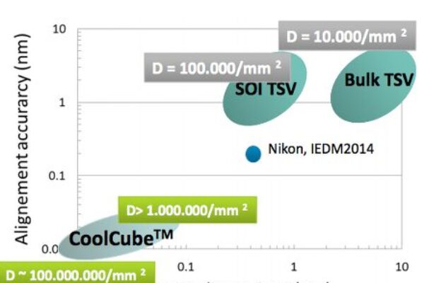
CoolCube is Leti’s sequential integration technology that stacks of active layers of transistors. It is enabled by halving the thermal budget for manufacturing transistors in second and higher layers while minimizing a sacrifice in performance. It also allows about 10,000 times higher density of interconnect than is possible with TSVs.
For CoolCube the next layer is produced on a second wafer and then transferred as a thin silicon wafer film peeled off from a wafer blank after planarization. Because the transferred film is so thin and optically transparent, well under a micron (compared to around 50 microns thin for thinned wafers), the new layer of transistors that are processed on top can be aligned to the bottom transistors with lithographic precision.
The process is good for stacked ICs as well as for the combination of heterogeneous process layers and the co-integration of sensors, MEMS with CMOS. "In heterogeneous integration, we expect CoolCube to be an actual enabler of smart-sensor arrays by allowing a close integration of sensors, detection electronics and digital signal processing," said Maud Vinet, Leti’s advanced CMOS laboratory manager. "In the digital area, we expect this 3D technique to allow a gain of 50 percent in area and 30 percent in speed compared to the same technology generation in classic 2D – gains comparable to those expected in the next generation," she also said.
The researchers already reckon that the co-integation of two layers of 14nm technology could create a denser FPGA than a 2D design in 10nm process technology. However that would require a fine-grained redistribution of the design so that memory would be substantially contained in one layer and logic substantially in another.
That requires supporting EDA software tools. "We are working with Mentor Graphics and a couple of other EDA firms on that," said Vinet.
The next steps will include: 1) Getting EDA firms to deliver tools to support 3D design with CoolCube; 2) Scaling up production from small test circuits to commercial scale circuits; and 3) Working on customer design, said Vinet. "The target is to intersect the 10nm process node late in 2017 early in 2018, " she added.
Related links and articles:
News articles:
Monolithic 3D integration beats next node
Qualcomm to leverage monolithic 3D for smartphones
 If you enjoyed this article, you will like the following ones: don't miss them by subscribing to :