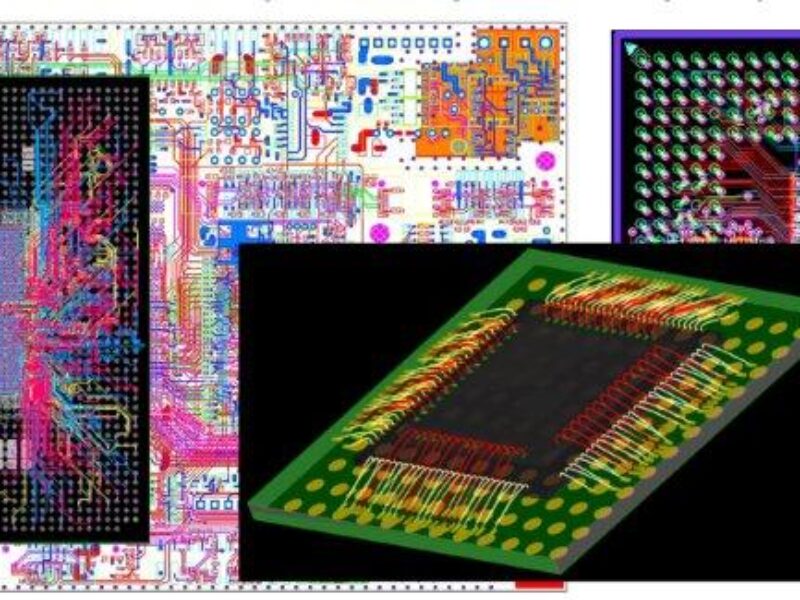
EDA visualises system designs from IC package to PCB
The Path Finder suite addresses the increasing design complexity of system on chip (SoCs) and multi-die packaging growth by providing the first new path-finding methodology that automates the planning, optimisation, and connectivity from a chip through multiple packaging variables, while targeting multiple and different PCB platforms.
Xpedition Path Finder provides designers with the ability to assemble and optimise complex electronic systems, and thereby enabling improved design, increased chip performance, and cost efficiency. This product, the newest addition to the Mentor Graphics Xpedition platform, supports a methodology that builds on layout data from IC and board design teams to guide and automate IC package selection and optimisation.
The Xpedition Path Finder suite provides a single environment that gives cross-domain design teams the ability to model every device/interface to the level of detail and accuracy they require. IC layout design data can be represented as a virtual die model (VDM), containing all of the IC-level detail specific to the co-design and optimisation process. Board design data can be modelled as individual interfaces or as complete designs. Packages can be built based on pin-array generation and manipulation capabilities, existing devices, and industry-standard formats. Cross-domain design teams can now make smart planning and optimisation decisions related to cost and performance of their IC package in context of the complete system.
Using the multi-mode connectivity environment, designers can capture and manage connectivity based on their preferred method; table-based, graphical schematics or automated. Cross-domain pin mapping and net combining can be managed in all modes of connectivity capture. In addition, users can perform rules-based pin/ball-out studies from their respective domains, by signal, bus or interface, visualising the impact across the complete system in real time. Path Finder also streamlines and automates the library development process, reducing a several-day task down to a few minutes.
The suite comprises a multi-mode connectivity engine and optimisation engine/editor, based on a physical layout tool with advanced routing technology. Features include:
- A correct-by-construction layout environment that enables designers to optimise performance and manufacturability on the densest designs populated by high-pin-count flip-chip BGAs. The core Xpedition layout tool provides: unique BGA breakout and escape algorithms coupled with support for complex microvia structures; shape-based, any-angle routing; plane areas that dynamically fill around traces and vias during editing; technology enabling efficient, concurrent design by large teams; and integrated RF circuit design and optimisation.
- Rule-based ball-out assignment, including an optimisation engine/editor for planning by bank, byte, reference voltage, clock domain, etc. – an intelligent way to show a ball map: simply create, import, and export.
- Single tool for multi-mode physical design (PCB, MCM, SiP, RF, Hybrid and BGA designs) that reduces design time orders of magnitude compared to other available products – using Microsoft-based Component Object Model (COM) automation for robust extension and customisation capabilities.
- Streamlined and fully automated library development.
- Virtual Die Model (VDM) to accurately capture IC layout (floor planning) design intent, facilitating WYSIWYG IC and package co-optimisation.
- Tight integration with 2D and 3D electro-magnetic (EM) and computational fluid dynamics (CFD) thermal analysis engines.
The Xpedition Path Finder suite is neutral with respect to EDA vendor, although it builds on other Mentor Graphics tools such as the HyperLynx signal and power integrity product, and 3D full-wave EM analysis tools, Xpedition layout technology, the FloTHERM CFD thermal modelling tool, visECAD/CAMCAD design comparison tool, and Valor NPI substrate fabrication checking tool.
Mentor Graphics; www.mentor.com/pcb/path-finder/overview
 If you enjoyed this article, you will like the following ones: don't miss them by subscribing to :