Improving receiver sensitivity: a story of ADCs and SiGe gain blocks
These noise sources can be the FPGA, the power supplies or the digital signals of the ADC itself. By designing a compact solution, barriers can be established between these noise sources and the analog input to reduce the noise coupled into the input network and the sensitivity of the system can be improved.
A compact solution may not be possible with high power amplifiers that can dissipate 4 W of power. With improvements to the noise performance of the system, low noise amplifiers with high linearity feeding a quiet ADC are required to maintain the desired sensitivity. Several advances in ADC design such as the new JESD204B standard have helped designers tackle design challenges that previously have limited receiver sensitivity. These advances, coupled with the new low power amplifiers, ultimately improve system noise performance.
Amplifier design challenges
Traditionally, high frequency applications used gallium arsenide (GaAs) or indium phosphide (InP) gain blocks to achieve high linearity and low noise. These gain blocks require voltages between 9-12 V which leads to 2-4 W of power dissipation per receiver channel.
Cooling the receiver board becomes a challenge and can degrade the performance of the system if left unmanaged. In battery powered or low voltage applications, traditional gain blocks may be a problem due to the high power dissipation.
Some gain blocks, also require some input or output matching circuitry that may change depending on the frequency range of interest. This reduces the total bandwidth that a single network can receive and increases the design time required to match the input network.
Additionally, the majority of these gain blocks are single ended, which is inherently imbalanced. Imbalance in any system will result in even order harmonics that need to be filtered to achieve good linearity. In many situations the second order terms may be close to the edge of the passband where the attenuation of the filter is low.
Since the second order harmonic distortion is not attenuated in these situations, the sensitivity of the receiver is reduced. By using a differential gain block to begin with, a balanced network can be designed, and second harmonic distortion is less of an issue.
Amplifier solutions
In order to reduce the power consumption of the GaAs gain blocks while maintaining good linearity and noise performance, a different, lower power process is needed. The LTC6430 is a differential gain block, designed in a low power silicon germanium (SiGe) process that minimizes the linearity and noise performance of high power gain blocks at a fraction of their power.
It operates from a 5 volt supply and draws only 160 mA of current, reducing the power consumption to less than 1 W. This reduction in power allows the LTC6430 to be used in low power, battery powered applications and in thermally sensitive applications in which a traditional gain block would not be appropriate due to the high thermal dissipation.
The LTC6430 is unconditionally stable with one matching network so all that is needed externally are DC blocking capacitors and RF bias chokes. This allows the LTC6430 to receive frequencies from 25 MHz to 1600 MHz with a single circuit.
This reduces the design time of the input network, allowing more time to be spent on other critical parts of the system. The simplicity of the LTC6430 matching circuit also reduces the required components as well as the complexity of the network between the ADC and amplifier, allowing for more room on the circuit board for barriers and vias to improve the results of the system.
The LTC6430 is a differential amplifier which naturally suppresses even order harmonics. The balanced nature of the LTC6430 produces cancellation of even order harmonics and improves the overall linearity of the system.
It also relaxes the attenuation requirement of the output filter between the amplifier and the ADC. The simplest possible balanced network between the ADC and amplifier will produce the best results by allowing room for barriers and vias to reduce interaction between the ADC and amplifier.
By reducing the filter requirement, the network uses fewer components and will provide a simple circuit to interface with the ADC. Since the LTC6430 has a differential output network, it can drive a differential ADC without a balun, further simplifying the input network of the ADC. With fewer components between the ADC and amplifier, the layout becomes easier. Also a more balanced network can be achieved to maximize the performance of the ADC.
ADC challenges
Noise in the receiver is not restricted solely to the amplifier and to channel noise. Noise present on the board from offensive signals can also be coupled into the ADC input network and gets digitized by the ADC. The magnitude of other sources of noise can be reduced with good layout techniques, but some is unavoidable.
One source of potential noise in the system includes the digital outputs of the ADC itself. With large voltage swings and high frequency content, the digital output signals can be coupled into the analog input and becomes redigitized, producing digital feedback.
Digital feedback can produce localized peaks up to 20 dB in the noise floor. Single ended CMOS signaling produces the worst digital feedback, since the higher the voltage swing the worse digital feedback will be.
Digital lines can also cause a more obvious problem: space constraints. With board space at a premium, multichannel ADCs with numerous output lines consume valuable board space. These buses of digital signals quickly become a nuisance, especially when routing takes them close to potentially sensitive circuitry like references, clocks or input networks. The closer these digital buses are to sensitive circuity, the more likely the digital noise will degrade system performance.
CMOS and LVDS traces also share another limitation: they are not DC balanced. This means that there is no mechanism for maintaining an average DC value. The fact that the average voltage can shift means that CMOS and LVDS signals cannot be transmitted through isolation barriers such as transformers, optical couplers, DC blocking capacitors, and other high pass devices.
In modern communications systems, antenna arrays are used for spatial diversity in the receiver. This allows for improved signal reception especially for weak signals or signals prone to fading. However, each additional antenna in the array requires another complete receiver chain.
As the number of antennas increases, there is a need for an increasing number of ADC channels. These ADCs need to be synchronized for maximum performance, which is not a trivial task. Variation in clock signals can cause the data to be interpreted incorrectly and degrades the performance of the system. Even with the best clock fanout devices there still can be skew between the various clock paths that cause skews in the digital data, which is challenging to sort out, even in the digital domain.
ADC solutions
By reducing the number of data lines and using digital signaling, the noise injected into the ground plane is dramatically reduced. The JESD204B standard uses pairs of CML data lines to transmit high frequency serial data. Depending on the sample rate, as few as one pair of lines is required. These pairs of transmission lines are differential in nature so there is a natural cancellation of fields, which reduces the effect of noise coupled into the ground plane.
Since the transmission of the data is serial and 8B/10B encoded, there won’t be repetitive patterns in the data that can produce frequency content on the ground plane eventually showing up on the analog input.
This greatly reduces the likelihood of digital feedback in the system. With less noise and high frequency content on the ground plane there is less energy that can be coupled to the analog inputs, which reduces the likelihood digital feedback.
With the data transmitted on serial data pairs, the routing of these traces becomes easier than routing a complete bus of parallel data. Since the data is transmitted using only one or two pairs of transmission lines, it becomes much easier to choose a path that is not surrounded by offensive signals. The transmission line pairs can be routed away from sensitive areas on the board.
A smaller routing area also allows for more vias to surround the transmission lines, which further reduces the likelihood that noise will couple onto the digital traces, or that noise from the digital traces will couple to the other sensitive circuits.
Another advantage of using 8B/10B encoding is that it is DC balanced. This is because the running disparity is used to maintain an equal number of ones and zeros over two alternate code groups, so the DC average of the signal is statistically zero. This allows a single pair transmission lines to be used with transformers, optical couplers, DC blocking capacitors, and other high pass devices.
By DC coupling, the signal can be transmitted across an isolation barrier through a transformer or optic coupler which will isolate the ground planes across the isolation barrier. This allows the sensitive receiver section to be electrically isolated from the noisy FPGA section, improving the sensitivity of the receiver by reducing the noise on the receiver section of the board. This allows the receiver section to be physically close to the antenna, and by using an optical connection, to have the FPGA section much further away, reducing the noise coupled from the FPGA into the receiver.
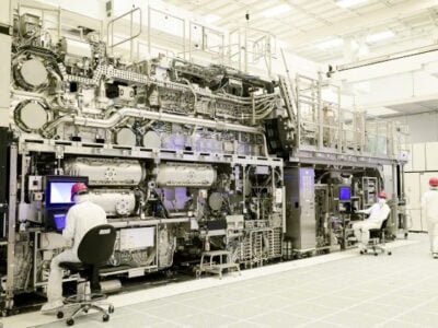
A significant advantage of the JESD204B standard is the ability to synchronize multiple ADCs to perform simultaneous sampling with multiple devices. This is done with a clock management device that provides a SYSREF signal to each of the ADCs and the FPGA, as shown in Figure 1.

Figure 1: Using SYSREF signal to synchronize two LTC2123s.
When this SYSREF signal is asserted, each of the ADCs and the FPGA align themselves to the SYSREF signal and the data from each of the ADCs is then aligned inside the FPGA. This allows simultaneous sampling of multiple channels of ADC data from different ADCs. This technique aligns ADC data and sample clocks making synchronization much easier. With the ADCs synchronized, the ability to receive data from multiple antennas becomes trivial, enabling the design of a more sensitive receiver.
Practical solution
The LTC2123 is a dual 250Msps 14-bit ADC with the JESD204B interface. It has an input bandwidth of 1250MHz, allowing it to be paired with the LTC6430 to create an excellent under- sampling receiver, capable of receiving frequencies above 1GHz. With the inclusion of the JESD204B output section, the LTC2123 simplifies board layout, reduces noise coupled into the ground plane, and allows the receiver to be isolated from the noisy digital portions of the system.
With the JESD204B circuitry, it becomes easier to synchronize multiple ADCs to have a large antenna array for antenna diversity applications. Since the noise figure of the LTC6430 is 3dB, the interface between the ADC and amplifier can be minimal.
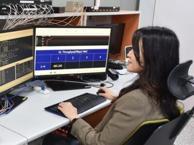
A typical circuit of the LTC6430 and LTC2123 is shown in Figure 2.

Figure 2: Interfacing an LTC6430 with an LTC2123.
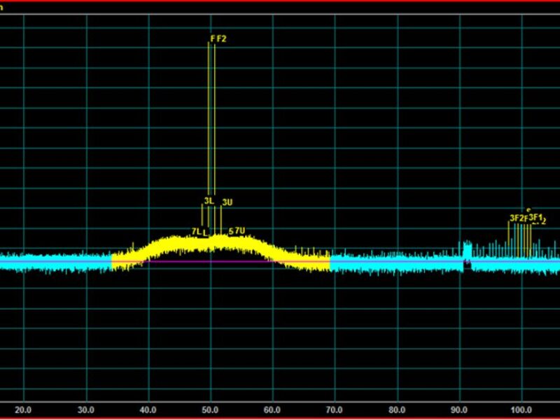
This allows the ADC and amplifier section to be compact, allowing for more barriers around the input network to further reduce the noise that can be coupled into the input network. The result of this combination is shown in Figure 3.

Figure 3: LTC2123 and LTC6430 two tone test — 250 Msps, F1 = 199.3 MHz, F2 = 200.3 MHz.
At 250 Msps, with tones at 199.3 MHz and 200.3 MHz, the 3rd order intermodulation distortion products are at -87 dBFS and the SNR is 68 dBFS. This performance is achievable over multiple receiver channels in a compact area because of the JESD204B interface and the lower power consumption of the LTC2123 and LTC6430.
The LTC2123 ADC and LTC6430 amplifier combination enables design of compact systems, ensuring maximum sensitivity in the receiver. By reducing power dissipation and the number of digital lines, the total solution size can be reduced, and barriers can be established around sensitive areas of the input network.
About the author
Clarence Mayott is Applications Engineer, Mixed Signal Products at Linear Technology – www.linear.com
 If you enjoyed this article, you will like the following ones: don't miss them by subscribing to :