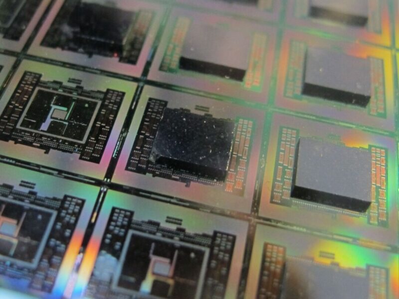
Intel calls for 3D IC
What Intel has proposed is essentially a shift towards other types of cost-saving technologies and process adoptions rather than relying on strict lithography improvement. Intel may be keeping its next-generation materials and lithography plans quiet, but the company does intend to push the envelope in other ways. 2.5D and 3D integration will be critical to the development of next-generation SoCs."
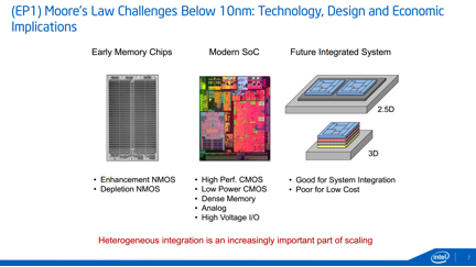
We clearly agree with Intel that the heterogeneous integration enabled by 3D IC is an "increasingly important part of scaling". This will become even more true as mobile and IoT markets increasingly will consume the lion share of the semiconductor business.
With respect to "Poor for Low Cost," this is only true for the TSV approach to 3D ICs. The following slide was presented in the recent 3D ASIP (2014) conference as the summary of "Will the Cost of 3D ICs Ever Be Low Enough for High Volume Products" presentation by Chest Palesko, a leading market researcher:
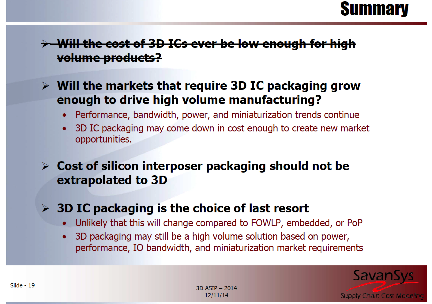
So, yes TSV-based 3D IC is "Poor for Low Cost".
But the other form of 3D IC, the Monolithic 3D, is the lowest cost path for future scaling!
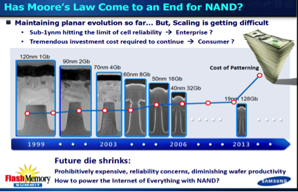
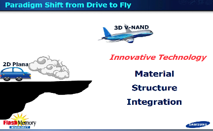
Samsung’s 3D NAND is an early example of monolithic 3D enabled scaling, being driven primarily by the push to increase bit capacity while reducing the cost per bit. Monolithically scaling up is now part of the International Technology Roadmap for Semiconductors (ITRS) and is being adopted by all NAND vendors. Samsung was the first to bring 3D NAND to mass production using the monolithic 3D approach:
The next market segment adopting monolithic 3D scaling is the image sensors as recently reported by EE Times: CMOS Image Sensors Surpassing Moore’s Law. Quoting: "imaging chips is downsizing the chip while simultaneously packing more pixels per unit size, thus one-upping processors and memory …
The CMOS imaging industry may make the 3-D TSV obsolete – before the processor and memory industry has even widely adopted it – by perfecting a wafer bonding technique that allows the connection between layers to be made with copper-to-copper (Cu-to-Cu) interconnects nearly as small as regular vias."
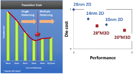
While still in the R&D phase, there is momentum building for monolithic 3D in logic too, as reported by CEA Leti’s work in collaboration with ST Micro, IBM, and Qualcomm. This was presented in the S3S (2014), 3D ASIP (2014), and IEDM (2014) conferences. The following chart was presented by CEA Leti and shows the cost reduction and performance improvements enabled by monolithic 3D scaling:
A recent validation of the unreasonable costs associated with dimensional scaling beyond 28 nm could be calculated from a recent EE Times article TSMC to Start 10nm in 2017, Closing Gap with Intel.
Quoting: "By the end of 2018, the company’s Taichung site will reach a monthly output capacity of 90,000 wafers at the 10nm and more advanced technology nodes, according to a report on the Chinatimes.com website. TSMC earlier this month said it would invest NT$500 billion ($15.9 billion) as part of an expansion at the Taichung site in central Taiwan." At two year’s depreciation, this represents $7,400 per wafer!!!
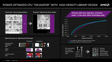
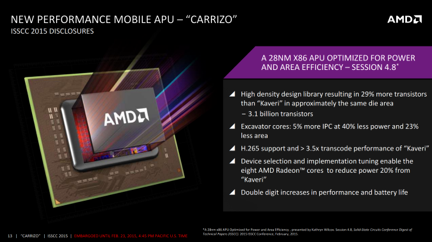
A misleading benefit which often gets attributed to dimensional scaling but has little to do with it, is the wide range of device improvements resulting from R&D efforts that typically coincide with the next scaling node. AMD’s recent presentation at ISSCC 2015 clearly illustrates this point by showing device improvements while still staying at the same 28 nm process node. As could be seen, major improvement in power, yield, and performance are possible over time without changing the technology node.
Monolithic 3D provides the industry many years of exponential integration growth while reducing cost and power by leveraging depreciation, learning curve, heterogeneous integration, low VT, SOI, shorter interconnections and many other powerful benefits of monolithic 3D, some of which are presented in our white paper The Monolithic 3D Advantage, monolithic 3D is far more than just an alternative to 0.7x scaling!!!
Until recently, the path to monolithic 3D required change to the front end-of-line process. An FEOL process change is always part of dimensional scaling, but is expensive, risky and in most cases done only by the leading edge companies. Now, as was presented in the recent IEEE S3S ‘14 conference, emerging precision bonders, such as from EVG or Nikon, enable a Game Changer for Monolithic 3D — a "true monolithic 3D IC without the need for a new recipe for transistor formation. The process could be adopted by any current fab providing very competitive costs for a range of product enhancements and offers a long term road map for better offerings by scaling up."
P.S.: A good conference to learn about this new scaling technology is the IEEE S3S ‘15, in Sonoma, on October 5th thru 8th, 2015. Two leading researchers from Berkeley and Stanford Universities will give invited talks presenting their work on advanced monolithic 3D integration technologies.
About the author:
Zvi Or-Bach is president and CEO of MonolithIC 3D Inc. – www.monolithic3d.com
Related articles:
Fan-out wafer level packaging fills gap to 3D, says Yole
TSVs to split more chips: re-integration is the focus
Manufacturers’ top tips to cost-effective 3D IC production
 If you enjoyed this article, you will like the following ones: don't miss them by subscribing to :