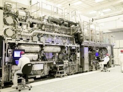
Samsung makes graphene at the wafer-scale
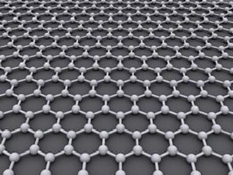
Graphene is an allotrope of carbon where the atoms are packed in a honeycomb lattice. The mobility of electrons in graphene is about a factor of 40 higher than that of silicon-based structures partly because of quantum mechanical effects of containing the electrons within two dimensions.
It is touted as being useful in the channel of high-performance transistors as well as in displays. However, the monolayer nature of the material makes it prone to damage during IC fabrication. In addition it has usually only been able to create graphene in small flakes limiting the possibilities of commercial use.
The authors reported in the journal Science Magazine the growth of wrinkle-free single-crystal monolayer graphene on a hydrogen-terminated germanium buffer layer on top of a silicon wafer. The diameter of the wafer was not disclosed in the abstract of the paper. The anisotropic twofold symmetry of the germanium (110) surface allowed unidirectional alignment of multiple seeds, which were merged to uniform single-crystal graphene with predefined orientation. In addition, the weak bonding of the graphene to the underlying hydrogen-terminated germanium surface enabled easy etch-free dry transfer of graphene and the re-use of the substrate for graphene production.
The research was funded by South Korea’s Ministry of Science, ICT and Future Planning (MSIP).
Related links and articles:
News articles:
TI growing large-area graphene
IBM researchers demo graphene IC on SiC wafer
Plastic Logic works on graphene for OLED displays
 If you enjoyed this article, you will like the following ones: don't miss them by subscribing to :