
Two-switch-quasi-resonant Flyback converter
The controller monitors the resonant ringing of the switchnode voltage and switches directly at the valley. This results in a lower voltage during the turn on of the MOSFET. Unfortunately this popular topology has some drawbacks. The input and output ripple currents of a QR-flyback are high because they are discontinuous. The primary and secondary windings are not coupled ideal.
This results in leakage inductance that stores energy during each cycle. This energy causes an overshoot (spike) of the switchnode voltage. To limit the peak voltage that the primary switch sees a snubber network is needed, that burns the energy stored in the leakage inductance, which lowers the efficiency. Another disadvantage of the standard flyback is that the MOSFET must withstand a very high voltage. During the demagnetizing time the drain-to-source voltage VDS of the MOSFET is equal to:
VDS = VBULK + VFLYBACK + VLEAKAGE
VBULK = voltage of the input capacitor
VFLYBACK = reflected output secondary voltage
VLEAKAGE = voltage overshoot due to leakage inductance
VLEAKAGE is typically in the range between 50V and 100V for offline designs.
The Two-Switch-Quasi-Resonant (2S-QR) flyback topology has the potential to overcome some of the drawbacks. First of all it recycles the energy of the leakage inductance. Secondly the maximum drain-to-source voltage of the MOSFET’s is equal or less the input voltage. The tradeoff for using this topology is not only the higher design effort, but also the obvious cost of the extra components. Two MOSFET’s (Figure1: Q1, Q2), two diodes (Figure1: D2, D3) and a driver-IC or gate-drive transformer are needed. It depends on the specific application if the 2S-QR topology is a serious alternative to the standard flyback.
Principle of Operation
The operation of the 2S-QR flyback topology is very similar to a traditional flyback. The main difference is that there are two MOSFET’s Q1 and Q2 (Figure 1) which turn on and off at the same time. When both MOSFET’s are on, the primary current starts at zero and rises to a peak value.

Fig. 1: Two-Switch-Quasi-Resonant Flyback
At turn off, the current transfers to the secondary (the energy is stored in the gab of the transformer) and the secondary current decreases to zero (called demagnetizing time), where it remains until the beginning of the next switching cycle. After the demagnetizing time no energy is left in the transformer but there is still energy in the parasitic switch node capacitance. The energy builds a resonant circuit with the primary inductance and the typically resonant ringing of the switch node voltage occurs. Modern QR controller monitors the ringing and switches directly at the valley. Diodes D3 and D2 (Figure1) clamp the voltage overshoot caused by the leakage inductance. The energy is returned back to the input capacitor and recycled.
Advantages of the 2S-QR vs. Standard Single Switch Topology
– Voltage rating requirements of the MOSFET’s (Figure 1: Q1, Q2) are lower. The drain-to-source voltage is equal or less than the input voltage.
– The energy stored in the leakage inductance is recycled.
Design Hints
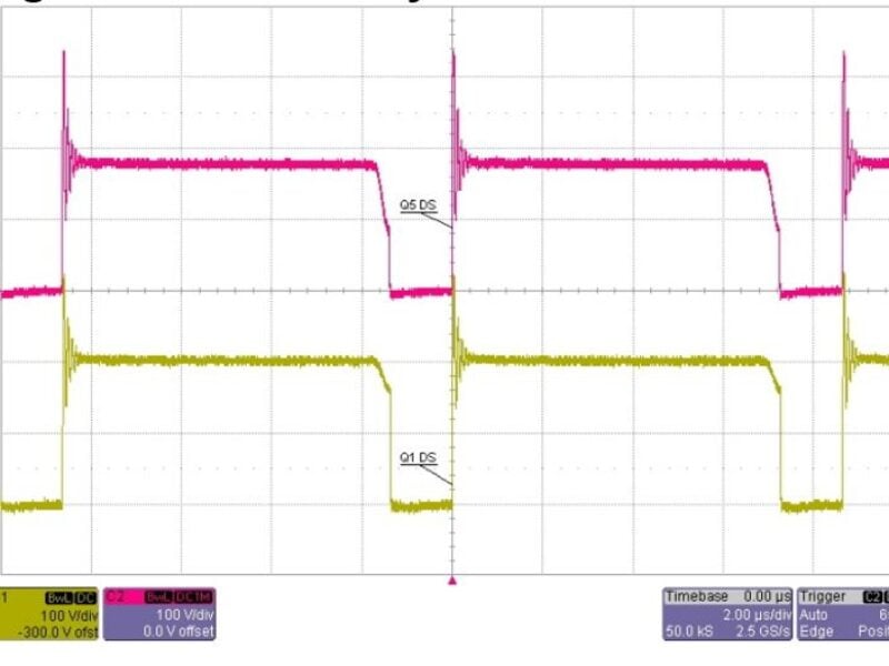
Please note that the overall voltage stress is not always divided equally over both MOSFET’s. The system is not always balanced. During the demagnetizing time the diode D3, the primary inductance and the diode D2 build a series connection to the input voltage. The voltage across the primary inductance is fixed, it is VFLYBACK. If there is an imbalance, the voltages across the diodes D2, D3 must not be equal.

Fig. 2: Balanced system.

Fig. 3: Imbalanced system.
Figures 2 and 3 shows the drain-to-source voltages VDS of the high side MOSFET Q1 (yellow) and the low side MOSFET Q5 (red) of an almost balanced and an imbalanced system. VDS can vary a lot, if the voltages across D2, D3 are not equal. The cause can be a delay of the high side gate signal amongst others. Adding a gate resistor for the low side MOSFET decreases the delay and could help balancing the system. But please note VDS can be as high as the input voltage for an imbalanced system.
Converting a standard QR flyback into a two switch QR flyback
The Texas Instruments reference design PMP10035 shows a 75W 2S-QR-flyback. The link https://www.ti.com/tool/pmp10035 provides the schematic, the testreport and the BOM of the design. It is possible to use a standard flyback controller (e. g. LM5023, UCC28600) for a two-switch flyback topology. The file (PMP10035 Schematic) provides the complete circuit.
The gate drive signals for the high side MOSFET Q1 can be taken from the gate drive pin of the controller U2 (LM5023, Pin2) because the drive signals for both MOSFET’s are equal. Problem is the high side position of Q1. A high side gate driver which can handle the maximum input voltage must be taken or an additional gate transformer (T1, PMP10035 Schematic) is needed. Care must be taken about the constant volt-seconds characteristic of transformers.
The duty cycle of the quasi-resonant flyback is natural limited because the next switching cycle cannot happen before all the energy stored in the transformer gap is delivered to the output. Nevertheless the gate drive transformer output pulses should be tested for all operating modes and conditions. If needed an additional coupling capacitor (PMP10035 Schematic, replacement of R2) and a simple diode clamp (PMP10035 Schematic, D3) on the secondary of the gate transformer can be used.
Maybe the input filter could be a little bit smaller for a 2S-QR-Flyback compared to a standard flyback because theoretically the currents spikes that result from charging the parasitic capacitance to ground tend to cancel. All other components of the circuit remain the same. The input and output capacitor, the transformer and the secondary compensation circuit are equal to the standard QR flyback.
Test results

Fig. 4: Efficiency
Figure 4 shows the efficiency of the reference design PMP10035. It is about 90% over a wide input voltage and output power range. Nevertheless a traditional QR flyback could reach almost the same efficiency. The benefit of the 2 switches and the recycled energy will be higher for an output power of more than 75W.

Fig. 5: Load transient response.
Figure 5 shows the load transient response. The open loop bandwidth is 1.6kHz. The over- and undershoot is about 200mV for a loadstep between 1 to 4A. The dynamic performance is the same compared to a standard flyback. There is no advantage or disadvantage between both topologies with regard to the load step behavior.
Conclusion
A standard QR flyback controller like the LM5023 can control the 2S-QR flyback topology. An additional high-side MOSFET including the driver circuit is needed. An output power of more than 75W will tap the full potential of this rarely used topology. Designers should think about this topology especially for an output power range between 100W to 200W and/or for high input voltages.
Visit Texas Instruments at https://www.ti.com/powerlab
About the author:
Florian Mueller is Systems Applications Engineer for Power at Texas Instruments – https://www.ti.com
 If you enjoyed this article, you will like the following ones: don't miss them by subscribing to :