Understanding DDR SDRAM timing parameters
To begin with, let’s first understand how different DDRs are rated or classified. If, we want to buy a DDR module from market, we have to consider many parameters like size, speed, timing specs, brand etc. So, we have many options to choose from. To have a better understanding of these ratings, let’s see how these are presented to the buyers. Below is the picture of a DDR SDRAM module.

As seen in figure 1, the module reads DDR3-1600MHz, PC3-12800. So, what does this mean? In DDRx-yyyy, ‘x’ represents the technology generation (example: DDR2, DDR3, DDR) and ‘yyyy’ represents the DDR clock rate or more appropriately the data rate. DDR (Double Data Rate), as the name suggests, transfers two chunks of data per clock cycle and hence achieve twice the performace as compared to the memory without this feature. It is for this reason that DDR are rated with twice the clock rate at which they function i.e. the data rate.
Usually, DDRx-yyyy convention is followed for the memory chips. But memory chips are not available as such. They are soldered onto tiny PCBs and are termed as memory modules, the speed of which is described as PCx-zzzz. In PCx-zzzz, ‘x’ represents the same technology generation and ‘zzzz’ is the maximum bandwidth i.e. maximum transfer rate in MBytes/s.
Maximum Transfer Rate = clock x number of bits / 8
Since memory modules transfer 64 bits at a time, the “number of bits” will be 64.
Therefore, the formula can be simplified as:
Maximum Theoretical Transfer Rate = clock x 8
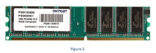
Also, one can see the operating voltage and the size of the module mentioned on the memory module. In figure 2, one can easily distinguish between the memory chips and the memory module. The tiny black entities embedded onto the green colour PCB are the memory chips and the complete integrated circuit is the memory module.
So, figure 1 throws out the following information. The memory module consists of memory chips which work at real clock of 800MHz i.e. its data rate is 1600MHz and supports a maximum possible data transfer rate of 12800 MB/s between the controller and the module. It has a capacity of 8Gb.
Now coming to the timing parameters, we notice 9-9-9-25 and 9-9-9-24 mentioned on the memory module in figure 1 and figure 3 respectively.
So, what exactly does the timing A-B-C-D (or sometimes CLA-B-C-D) mean? It’s intriguing how sometimes two memory modules with same maximum transfer rate, running at same clock frequency achieve different performances. Its because of different timing parameters. The memory timings are given through a series of numbers; as in figure 3, 9-9-9-24.

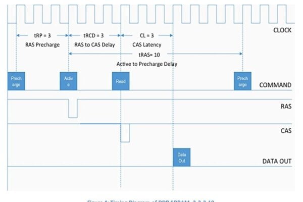
These numbers are a measure of the time the memory chip takes for performing internal operations. It indicates the amount of clock cycles taken by the memory to perform the internal operations. The smaller the number, the faster the memory. The operations that these numbers indicate are as following: CL-tRCD-tRP-tRAS(-CMD). To understand these operations better let’s first understand the SDRAM access procedure.
DDR SDRAM access:
Memory is organized into a grid-like pattern, with "rows" and "columns". The data stored comes in blocks and is defined by the coordinates of the row and column. The steps for the memory controller to access data in SDRAM follow in order:
First, the SDRAM is either in idle state or executing the previous operation.The controller issues the "active" command. It activates a certain row, as indicated by the address lines, in the SDRAM chip for accessing. This command typically takes a few clock cycles. After the delay, column address and either "read" or "write" command is issued. Typically the read or write command can be repeated every clock cycle for different column addresses (or a burst mode read can be performed). However, the read data isn’t available until a few clock cycles later, because the memory is pipelined. When an access is requested to another row, the current row has to be deactivated by issuing the "precharge" command. The precharge command takes a few clock cycles before a new "active" command can be issued.
Now we can study the detailed definition of various timing parameters.
CAS Latency (CL) : CAS Latency (Column Access Strobe Latency), also known as “Access Time”, is the most important memory parameter and is the first of the series of numbers. It is the delay time between the moment a memory controller tells the memory module to access a particular memory column on a RAM memory module, and the moment the data from given array location is available on the module’s output pins. In DDR SDRAM it is specified in clock cycles, while in asynchronous DRAM it is specified in nanoseconds.
RAS to CAS Delay (tRCD): ‘tRCD’ stands for row address to column address delay time. Inside the memory, the process of accessing the stored data is accomplished by first activating the row then the column where it is located. tRCD is the time required between the memory controller asserting a row address strobe (RAS), and then asserting a column address strobe (CAS) during the subsequent read or write command. The lesser this time, the better it is, as the data will be read sooner.
RAS Precharge (tRP): Whenever a new row is to be activated for the purpose of accessing a data bit, a command called “Precharge” needs to be issued to close the already activated row. RAS Precharge time, tRP is the number of clock cycles needed to terminate access to an open row of memory, and open access to the next row.
Active to Precharge Delay (tRAS): After an “Active” command is issued, another “Precharge” command cannot be issued until tRAS has elapsed. So, tRAS is the minimum number of clock cycles needed to access a certain row of data in the memory between the data request (Active) and the Precharge command. Basically,
this parameter limits when the memory can start reading (or writing) a different row.
Note: All the four parameters work with memory real clock i.e. half the rated clock. A memory with CL=4 need not be slower than the one with CL=3. It all depends on what clock frequency both of them work and accordingly, absolute latencies can be calculated for each of the two.
For better understanding, the timing diagram of a memory with timing parameters 3-3-3-10 (assumed) is presented in figure 4.

To conclude the article, we can summarize the timing parameters as below:
· CAS Latency (CL) is the time it takes to read the first bit of memory from a DRAM with the correct row already open.
· The time to read the first bit of memory from a DRAM without any active row is tRCD + CL.
· The time to read the first bit of memory from a DRAM with the wrong row open is tRP + tRCD + CL.
· The number of clock cycles required between an “Active” command and issuing the “Precharge” command is tRAS.
You can reach the authors at:
Deepak Kumar Behera (deepak@freescale.com)
Sumit Varshney (B17255@freescale.com)
Sunaina Srivastava (B18098@freescale.com)
Swapnil Tiwari (B36245@freescale.com)
 If you enjoyed this article, you will like the following ones: don't miss them by subscribing to :