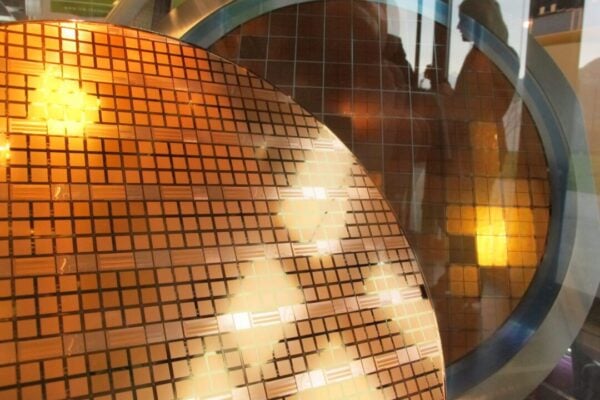
Developing and strengthening 3D IC manufacture in Europe
“There were only local summits so far”, explained Heinz Kundert, President of SEMI Europe, “and this is truly the first time that a conference on 3D Through Silicon Vias (TSV) receives such a global attention, from key European players but also from outside Europe”. “A lot has been spent on R&D and Europe has very good universities, but we also need to maintain a critical mass in IC manufacturing in Europe, otherwise, we could lose our knowhow and critical edge” continued Kundert.
There are many issues that need to be addressed for 3D IC manufacture, and now is the chance for Europe to bring IC production back from Asia, according to Kundert. “In highly automated fabs, it may no longer be economical to produce ICs in Asia, especially with all the associated costs of staff travel, and complex machine parts imports/exports”, Kundert highlighted. In fact, there is a reverse relocation trend happening, from Asia to Europe and to the US.
As a global semiconductor industry association, SEMI Europe’s role is also to ensure that its members can compete with the Asian and American industry on fair grounds, with the same sort of tax reliefs and energy deals, but also with more education in electronics.
In that sense, the European 3D TSV Summit’s recent success helps raise the semiconductor industry’s visibility and get the message across the European Commission. SEMI Europe documents the industry and negotiates with the European Commission on behalf of its members.
“The European Commission has now understood that semiconductors represent a key enabling technology for growth in Europe, and this needs to be supported not only with spending in R&D, but also by financing pilot production lines. We are here to raise the issues and to provide a single European strategy for the semiconductor industry, comforting our members that they have a future in Europe” concluded Kundert.
Solutions from 2.5D interposers to 3D ICs
Although the latest developments around through-silicon vias are aimed at improving direct chip-to-chip connectivity and true 3D IC designs, so-called 2.5D interposers where several chips are connected through an interposer rather than directly using TSVs still have a future. In fact in the next five years, market and technology analyst for advanced packaging at Yole Développement Lionel Cadix expects 2.5D interposers with system partitioning applications to be the biggest drivers for the volume adoption of 3D IC technology.

A typical implementation of a system-partitioning interposer as illustrated by Yole Dévelopment.
For the global production of TSV chip wafers, the analyst forecasts an impressive compound annual growth rate (CAGR) of 56% between 2012 and 2017, with 2.5D interposer platform wafers shipping at nearly double that rate, growing from less than 100,000 12-inch equivalent wafers today to over 2.5 million in 2017. This is explained by the increasingly complex role that interposers could play in system-partitioning, not only enabling the integration of logic ICs with memory ICs, but possibly allowing designers to mix digital and analog ICs like in a SiP but with better electrical and thermal performances. From a thermal standpoint, 2.5D integration enables similar benefits to those of 3D integration without the thermal drawbacks of overheating, highlighted Cadix.
In such system-partitioning, the interposers can act as heat spreaders across the package surface area. 2.5D system-partitioning interposers will often offer a cost effective alternative to all 3D IC design by enabling the use of optimised technologies for each IC (memory, logic, analog, MEMS) with higher yields. This also includes the possibility to cut down large logic chips into several circuits with higher frontend manufacturing yields. The analyst noted that beyond eight cores, processors will lose performance benefits if designed in a 2D configuration. " 2.5D interposers offer a solution to the fundamental bandwidth bottleneck of 2d architectures and will soon be mandatory for increasing the performance of high performance computers " he concluded, taking the example of Xilinx’ Virtex 7 HT (four slices processed at 28nm on a 25x31mm 100µm thick silicon interposer) or IBM’s next Power 8 multi-core CPU to be based on 2.5D interposers.
According to Yole développement, the 3D TSV market could reach USD 40B in 2017, growing more than 10 times faster than the global semiconductor industry. And 2013 could well be the turning point with the introduction of micron’s Hybrid memory Cube.
In his presentation, CEA-Leti’s CEO Laurent Malier acknowledged the importance of what he calls smart interposers, an all-encompassing expression for what could include thermal dissipation solutions, and die substrates with integrated passives, photonic interconnects or even active silicon interposers.
On CEA-Leti’s 2015 roadmap, the active interposer concept would support SoC partitioning into several dies, with different technology nodes. This enables the faster introduction of new processes, using small dies manufactured at a better yield. The active silicon interposer would integrate not only interconnects but also analog functions, memory control and I/O peripherals. So far, the lab has demonstrated direct face-to-back integration (wideIO memory on a SoC) and face-to-face chip integration (a logic chip on an analog one at 65nm). The ultimate goal would be to achieve modular and stackable logic dies (logic-on-logic), but this would require a 3D network-on-chip (NoC). By 2014, Malier hopes to be able to demonstrate a 3D asynchronous NoC that would support fast serial links and full asynchronous logic to avoid clock distribution issues across the stack. The network would include 2D and 3D NoC routers distributed throughout the 2D logic dies. Further on the radar, Malier also mentioned prospective work on a 3d cache memory concept to be stacked on a manycore processor. This would rely on a non-uniform memory architecture capable of splitting cache into multiple banks interconnected with a NoC. The 3D stacking would add flexibility for capacity, high bandwidth and fault tolerance. Such an architecture would require a 10µm TSV pitch and in excess of 10,000 TSVs per chip, compared to the relatively large grain 3D partitioning (50µm TSV pitch) required for logic-on-logic solutions.

On CEA-Leti’s 2015 roadmap, the active interposer and the TSV technology that must be scaled down for such solutions.
Because each TSV also requires a buffer or keep-away zone (to limit unwanted capacitive couplings and mechanical stress), TSVs need to shrink to achieve surface (silicon real estate) cost reduction. Towards that goal, the lab has demonstrated high-density low diameter TSVs (3µm) across 15µm of silicon. In the future, thermal hot spots could be addressed with integrated graphite heat spreaders, but also with phase change materials for dynamic temperature smoothing, and possibly long distance heat dissipation using a cooling fluid through micro-channels.
The challenges for stacking dies into true 3D ICs are not just about process control, TSV density and 3D routing, thermal issues could become the real bottleneck. First, thermal models and design rules must be established. Xilinx’ senior director for packaging and advanced technology development, Suresh Ramalingam shared his experience on the Virtex-7 2000T, a 2.5D device that combines a whopping 6.8B transistors across four FPGA sub-dies on a 4-layer metal Si interposer with over 10,000 inter-die connections.
Ramalingam insisted on the need for co-design, optimizing dies for extra performance through homogeneous and heterogeneous 3D integration. “With 3D integration using an active die as the carrier (instead of an interposer), you have to decide which chip must go on top”, he said. Ramalingam’s short answer is that the high performance chip should go on top for thermal and TSV process availability (smaller diameter), whilst the bottom die, designed with a more mature technology node should support power TSVs for the top die.
Again, it is critical to address the stacked thermal flux with good floor-planning. This calls for multi-physics, multi-die analysis and thermal modelling based on vertical hotspots for which the tools are yet to come, commented Uwe Knöchel, a researcher at the Fraunhofer IIS, Design Automation Division.
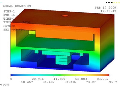
Thermal flux modelling for a 3D IC stack using Fraunhofer IIS’ internal multi-physics tools.
In fact, “3D IC stacking opens such a big design space that a new class of tools are needed to decide the best design approach. This is particularly difficult because these multi-physics, multi-scale designs exceed the capacity of current simulators”, Knöchel added. You must interface very different tools in order to achieve a thermal-aware floor-planning, for complex designs, Knöchel had to rely on in-house academic solutions.
Defining a process flow
Eric Beyne, director of advanced packaging at imec gave us some insights on the manufacturing supply chain needed for a unified 3D IC design flow across foundries and package manufacturers. It could be split into front-end, middle-end and back-end process modules. In the front-end module where the semiconductor device TSVs after the Front-end-of-Line (FeoL) device fabrication, but before the back-end-of-line (BeoL) interconnects.

imec has demonstrated copper vias with an aspect ratio of 10 (5µm diameter, 50µm deep).
The mid-end process module would include wafer to carrier bonding/debonding, thinning, then backside TSV reveal and passivation, and the addition of a redistribution layer, microbumps and copper pillars. The back-end process would then consist in the actual 3d stacking of the prepared dies and wafers, either die-to-die or die-to-wafer. The consensus in the industry seems to be that TSVs should be scaled down for cost and capacitance reduction.
Vertically,this can be achieved by thinning the wafers and by manufacturing high aspect-ratio TSVs. Imec has demonstrated copper vias with an aspect ratio of 10 (5µm diameter, 50µm deep) obtained in a single litho-step.
Further on its roadmap, the Belgium university campus sees 30µm deep TSVs with a diameter of only 2µm to be integrated with advanced device nodes.
imec has also demonstrated thin wafer handling (thinning down to 50µm) with backside passivation and copper via exposure.
An interesting contribution from Jurgen Wolf, Department Head of HDI WLP/ASSID at Fraunhofer- IZM / ASSID was to showcase the institute’s capabilities for etching TSVs with an aspect-ratio of over 12 (10µm/120µm and 5µm/60µm+) and the development of nanoporous gold bumps for chip to substrate bonding. The new Ag/Au alloy chemistry used for bump deposition can be used in a conventional Au bumping process flow. The nano-sponge is obtained through de-alloying by wet etching the aluminium. This sponge-like gold bumps have an average pore sizes adjustable from 20nm up to 500nm and are fully compressible and able to compensate topography issues on chip and substrate, which can also be an issue for die-to-die and die-to-wafer stacking.

Nano-porous gold bumps for chip to substrate bonding by Fraunhofer- IZM / ASSID
Frederic voiron, senior r&d engineer at IPDIA gave a good illustration of what 2.5D passives interposers could bring into the equation. Thanks to his company’s passive integration connecting substrate (PICS-IPD), hundreds of passive components could be integrated into a single silicon interposer, he said, claiming the world record of capacitance density in silicon, with 250nF/mm2 in production (on 100 µm wafers) and 500nF/mm2 tested and demonstrated.

IPDIA’s passive integration connecting substrate (PICS-IPD) with its embedded capacitors: concept and micrograph.
The technology could be combined with TSVs to build system-in-package solutions or even passive dies stacking for volume-constrained application.
Thorbjörn Ebefors, Chief Technologist, co-founder and VP of R&D at Silex Microsystems had a particular eye on TSVs for MEMS solutions. For MEMS applications, TSVs are used either through the sealing cap or through the bulk substrate and at much lower densities, typically 1 to 10 TSV/mm2. They allow for compact MEMS-ASIC packaging, either wirebond or flip chip. The TSVs can be built directly into the MEMS substrate, eliminating the need for an organic substrate or interposer altogether (all-silicon package). Silex Microsystems offers two types of TSV technologies: the Sil-via rigid interposer developed in 2003 across the full wafer thickness and a more recently developed met-via baseline process released in 2010, for TSVs through the MEMS cap. The ability to create TSVs through full wafer thickness means the interposer can be the package, using existing wafer processing, without exotic thin wafer handling. Again, the silicon substrate can be “functionalized” with passive or active elements. For example the MEMS cap wafer could integrate vertical capacitors, but also inductive coils with a magnetic core for driving the MEMS structures. The latter can be realized as a combination of Met-via TSVs and copper-traces on the wafer’s surfaces with a layer of FeNiCo alloy trapped into the windings.

Silex’MEMS cap wafer could integrate vertical capacitors, but also inductive coils with a magnetic core for driving the MEMS.
3D stack testing
Working with known-good-dies won’t be enough to secure high 3D IC yields, and new testing strategies need to be developed. “Design-for-test is the way to go”, was the main message from Brandon Wang, Director 3D IC and Advanced Technology Product Management at Cadence Design System. First you need the tools for design partitioning, at different technology node for each die, then you must look at the die orientation and stacking orders, and last you must analyse performance (delay, latency), power distribution (thermal issues) and mechanical stress.
This calls for a co-design between the package, the IC stack and the interposer for optimized TSV and bump locations, cross die bump optimization and best power plans. This is when you must design the interconnects and die-internal circuitry to ensure test access at the bottom die, in a way that allows test stimuli and response propagation up and down through the final 3D stack. This systematic approach requires new layout rules. In collaboration with imec, the EDA company has implemented and validated an automated 3D design-for-test (dFt) solution to test logic-memory interconnects in DRAM-on-logic stacks.
Based on Cadence Encounter Test technology, the solution was verified on an industrial test chip containing a logic die and a JEDEC-compliant Wide-I/O Mobile DRAM (on an interposer). The solution supports post-bond testing of the interconnects between the logic die and the dram stacked on top of it. It also includes the generation of dram test control signals in the logic die and the inclusion of the dram boundary scan registers in the serial and parallel test access mechanisms (tams) of the 3d test architecture. The inserted 3D dFt wrapper IP had a negligible impact on die area, at about 0.3% of total circuit silicon footprint.
Wang also disclosed a thermal analysis flow and an IR drop analysis flow where all the micro-bumps and TSVs are modelled as RC or RLC networks while all the chips are analysed at the same time for accurate results.
So what about accessing these tiny test pads at the bottom of the stack? Senior director for Business development at advantest, Gary Fleeman hinted at MEMS-based micro-probe tips that would not break the thin wafers nor dig marks on the copper traces. Advantest is evaluating the InfinityQuad probe technology developed by Cascade Microtech, with monolithically fabricated tips at a 40 µm pitch, with a positional accuracy to within 1 µm and excellent planarity (a prerequisite for good contact yield).
Another MEMS-based approach under development from sister company touchdown Technologies relies on a swinging probe tip that would yield lower tip forces (under 1 gram-force) for a lesser pad damage. in principle, such approaches would be scalable to finer pitches.

New MEMS-based micro-probe tips from TouchDown Technologies could rely on a swinging probe tip to yield lower tip forces for a lesser pad damage.
 If you enjoyed this article, you will like the following ones: don't miss them by subscribing to :