ESD Standard Vis a Vis IoT applications
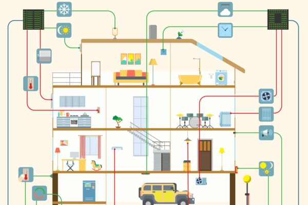
The home of the future – smart appliances that help you track your fresh food purchases as well as advising what and how to cook your meals; smart lighting systems that sense the ambient light conditions and adjust brightness accordingly or shift their color palette to change the mood; smart climate controls that ”learn“ the habits of the residents to most efficiently use energy to heat or cool; smart gateways that manage data, entertainment and communication; smart wearables and clothing that provide feedback on fitness activity and health parameters and that track those metrics to allow an individual to adjust their behavior to get positive health benefits; smart vehicles and traffic systems that improve traffic flow patterns and that make road travel safer.
Sounds pretty good! This vision of a future with a fully functional Internet of Things is quite bright with many new capabilities that allow individuals to take more control of their surroundings with respect to efficiency, enjoyment and even for better health. Similarly, smart factories will improve their owners‘ ability to control the process, quality and cost more effectively through coordinated manufacturing, measuring and analyzing systems.
What do all these systems have in common, and more importantly, what does it take for them to be considered ”smart“? Communications! The ability to receive and transmit information is crucial to systems being considered for inclusion in modern, smart systems. But, these information paths also provide an entry way for electrical threats to enter the system and damage it. Specifically, the most common threat is ElectroStatic Discharge (ESD). Any time that a cable makes contact with a connector, or a person makes contact with an electronic system, there is a possibility of electrical charge transfer.
For system designers, this provides a threat to the integrity and reliabilty of their piece of the Internet of Things. As the charge spreads out on the surface of the application, some or most of the charge can make its way through the connector (or other interface) and into the sensitive circuitry inside. In order to help system designers understand how to harden their product against ESD, a number of Standards have been developed, with the goal of ensuring the reliability of the integrated circuits, and thus, the application itself.
These Standards are designed to help at different levels of the electronic ecosystem:
- Human Body Model:It is based on a model of discharging a 100pF capacitor through a 1,500Ω resistor.Test voltages of 500V to 1,000V are typically used.This test is performed on integrated circuits to ensure they can survive the wafer fab and assembly processes.

-
- IEC 61000-4-2:It is based on a model of discharging a 150pF capacitor through a 330Ω resistor.Test voltages up to 8kV (contact) and 15kV (air) are typically used. This test is performed on finished product to ensure that it will survive interactions with end users.

- ISO 10605:This test is specific to the Road Vehicle market and is based on a model of discharging a 330pF or 150pF capacitor through a 330Ω or 2,000Ω resistor.The test depends on whether the circuit under test is accessed inside the vehicle, or from the outside of the vehicle.Similar to the IEC 61000-4-2, it is performed on finished vehicles to ensure that contact from drivers, passengers, assembly personnel and technicians will not damage the circuits.In addition, electronic modules that will be integrated within vehicles are tested prior to installation.
- DO 160, section 25: This test is specific to airborne equipment and is based on the same test model as the IEC 61000-4-2; and uses the 15kV air discharge method.The test is performed on finished product and is meant to replicate that action of people accessing the various circuits and applications inside and around the avionics equipment.

After reviewing these test Standards, there is a very clear conclusion. The severity of the ESD models for the completed products are very different to that of the Human Body Model (HBM). In short, the ESD testing that is done on integrated circuits is considerably weaker than the testing done at the application or module level. There is a mismatch, or gap, in the test levels and this means that even though an IC can survive the HBM testing, it may be very easily damaged once it is exposed to ESD levels expected in an application. Put another way, IC-level ESD capability does not infer robustness at the application level.
In order to compensate for the fact that ICs can be damaged by the ESD levels that will be experienced inside the application, board-level ESD components should be added to the circuit. These components act as shunt elements that divert the ESD energy from the I/O or power line to the ground plane or neutral line. The on-chip ESD structures of the IC can then handle the remaining energy and protect the funtional core IC (processing, memory, etc.).
Sounds easy? Well, in the past, it would have been a routine exercise. The ICs from a decade ago were inherently robust due to the large size of the IC structures. However, today, technology in production is now at 28nm, and in the future will move to 18nm and even 12nm processes. For these ICs, the PCB-level ESD components must shunt as much of the ESD energy as possible to ensure IC survival. Many manufacturers name this parameter the dynamic resistance. It must be as low as possible to ensure the clamping voltage is equally low to protect the IC.
A quick note on ESD protection technologies. There are three generally-accepted technologies, each with their own advantages. Polymer ESD suppressors typically have the lowest capacitance so are very compatible with high-speed data lines. But they tend to have the highest dynamic resistance. Ceramic ESD suppressors (multilayer varistors) are typically discrete components in standard sizes from 0201 to 1206, and can handle both ESD and surge transients. Semiconductor-based ESD components are available in a wide range of form factors and tend to have the lowest dynamic resistance value.
So, what is a design engineer to do? Fortunately, organizations like the Industry Council on ESD Target Levels and companies like Littelfuse provide help to the design community. The former is an industry group of professionals with representatives from IC makers, test equipment suppliers, Consumer, Telecom and Automotive manufacturers and component suppliers. Working together, they have created guidelines for understanding the relationship between the IC-level ESD Standard and the application level Standards. More importantly, they also provide a process for designing systems such that they will survive severe ESD transients in the field, taking into account the limitations of the on-chip ESD capabilities of modern ICs. They have named this approach as System-Efficient ESD Design.
The System-Efficient ESD Design (SEED) methodology takes into account a number of different criteria in order to model the IC and the PCB-level ESD protection device in order to simulte the effect of an ESD pulse hitting this ”system“. The purpose is to determine whether the tested IC will survive an ESD pulse based on its on-chip protection as well as the parameters of the PCB-level ESD components. It is meant to de-mystify the ESD design process and provide a consistent framework for working through the ESD design process. For a better understanding of this process, it is suggested that the reader reviews the White Papers from the Industry Council on ESD Target Levels; they are publicly available on the Internet.
For those designers who do not have the time to perform this research, Littelfuse has partnered with Pragma Design, Barth Electronics and WebSIM to create an online tool that can be used to explore and understand this process. The Littelfuse iDesign™ Online Simulation tool provides a background on the process and then helps the designer to input/select the needed parameters to run the simulation. It takes into account key parameters of the IC as well as those of the intended ESD protection component. The result of the simulation shows the likely and best case system-level ESD robustness. It can be used to understand how the selection of different ESD components affects the system-level capability; also to identify potential solutions that can be tested in the designer’s application.
The Internet of Things promises to provide a wide range of new capabilities with respect to monitoring and quantifying systems our environment and even ourselves. However, these benefits are threatened by our interaction with the IoT systems due to ESD transfer. By recognizing this early in the design process, engineers can improve their design and also their time to market by avoiding failures that would be found later in the design process. In addition, organizations like the Industry Council on ESD Target Levels and companies like Littelfuse provide aid in the form of information and design tools to make the process to achieving ESD immunity easier and quicker than in the past.
About the author:
Jim Colby is Manager of Business and Technology Development, Semiconductor Business Unit at Littelfuse – www.littelfuse.com
 If you enjoyed this article, you will like the following ones: don't miss them by subscribing to :