III-V FinFETs on 300mm silicon wafers at imec
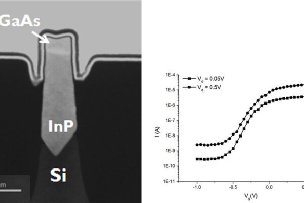
The Belgian research centre says it has demonstrated the first III-V compound semiconductor FinFET devices integrated epitaxially on 300mm silicon wafers, through a unique silicon-fin-replacement process. The breakthrough not only enables continual CMOS scaling down to 7nm and below, but also enables new heterogeneous system opportunities in hybrid CMOS-RF and CMOS-optoelectronics.
“To our knowledge, this is the world’s first functioning CMOS compatible III-V FinFET device processed on 300mm wafers,” stated An Steegen, senior vice president core CMOS at imec. “This is an exciting accomplishment, demonstrating the technology as a viable next-generation alternative for the current state-of-the-art Si-based FinFET technology in high volume production.”
Ever growing demands for bandwidth and connectivity, will drive the continual need for software and hardware advancements; at the core of the hardware will be new process technologies that allow for more power-efficient CMOS transistors and increased integration, enabling a higher level of functionality. This prompts process technologies that enable heterogeneous devices spanning operating ranges for targeted circuits, maximising the system performance.
Aaron Thean, director of the logic R&D at imec commented: “During the last decade, transistor scaling has been marked by several leaps in process technologies to provide performance and power improvements. The replacement of poly-silicon gate by high-k metal-gate in 45nm CMOS technology in 2007 represented a major inflection in new material integration for the transistor. The ability to combine scaled non-silicon and silicon devices might be the next dramatic transistor face-lift, breaking almost 50 years of all-silicon reign over digital CMOS. This work represents an important enabling step towards this new paradigm.”
At the finest grain, co-integration of high-density heterogeneous transistors has been challenged by the ability to combine disparate materials and structures while maintaining low enough complexity and defectivity. Imec’s breakthrough process selectively replaces silicon fins with indium gallium arsenide (InGaAs) and indium phospide (InP), accommodating close to 8% of atomic lattice mismatch. The new technique is based on aspect-ratio trapping of crystal defects, trench structure, and epitaxial process innovations. The resulting III-V integrated on silicon FinFET device shows an excellent performance.
Imec’s research into next-generation FinFETs is performed as part of imec’s core CMOS program, in cooperation with imec’s key partners including Intel, Samsung, TSMC, Globalfoundries, Micron, SK Hynix, Toshiba, Panasonic, Sony, Qualcomm, Altera, Fujitsu, nVidia, and Xilinx.
Imec; www.imec.be
 If you enjoyed this article, you will like the following ones: don't miss them by subscribing to :
eeNews on Google News


