The influence of contaminant residues on PCB Spot Weld and Discussion on Cleaning Craft
Although the soldering craft of low residue and no-clean is well utilized by traditional Surface Mount Technology (SMT), in the products with high reliability, the structure densification of products and the miniaturization assembly of components make it increasingly more difficult to reach the suitable cleaning grade with an increase of product failure led by the cleaning problem. This passage will briefly discuss the influence of contaminant residues on PCB spot weld and some problems concerning cleaning.
● The Influence of Contaminant Residues on PCB Spot Weld
a. Electrochemical Migration
ECM, short for Electrochemical migration, refers to ion migration by means of some medium such as flux leftover under the influence of electromagnetic field. For PCB products, with the change of the environmental humidity, some ionic contaminants in the flux residue such as the active agent and salt will be changed into electrolytes, leading to the feature change of spot welds. When these PCBs are working, under the condition of stress voltage, short cuts will possibly take place between spot welds, causing intermittent faults that decrease the reliability of PCBs.
This process is comprised by three steps: path formation, initialization and arborized crystal generation. The path formation starts with the dissolution of metal ion in the electrolyte that is a kind of weak acid formed by the combination of chlorine and bromine residue in the flux and the water in the air. When metal is dissolved in the weak acid, metal filament will be generated. Therefore, the elements including ionic leftover, voltage deviation and humidity must be required to implement the mechanism of the electrochemical effectiveness. Besides, the electrochemical effectiveness is also influenced by temperature, humidity, offer, conductor material, conductor spacing, contaminant type and quantity.
b. Creep Corrosion
Creep corrosion refers to the phenomenon that the sulfide crystal of copper or silver is generated on the surface of PCBs. Different from electrochemical migration, just the existence of contamination source and moisture in the environment is capable of leading to the creep corrosion, without the need of voltage difference. When the sulfur in the air combines with the copper or silver on PCBs, copper sulfide or silver sulfide will be generated.
These chemical compounds such as copper sulfide and silver sulfide will grow towards any direction, making fine leads open or short cuts between spacing leads, which will finally result in the bad quality of PCBs. With the PCB size becoming smaller and components miniaturized, the risk of this type of corrosion will definitely improve. Creep corrosion mostly occurs in the fields of industrial control electronics and aerospace because of the more existence of contamination gas in their ambient air.
Another reason lies in the HASL implementation on the surface of previous PCBs whose outside copper foil is protected by tin lead. However, with the development of lead-free craft, materials with copper or silver are used in PCB fabrication, welding and plating. Once the wetting doesn’t reach the grade in the process of soldering, some copper or silver will be exposed to the air and when the environment becomes bad with the influence of moisture, the risk of creep corrosion will increase greatly.
c. Tin Whisker
Tin whisker is the main concern of professionals. Through a large amount of research based on the chemical and physical parameters generated by tin whiskers, experts indicate that the alloy with tin proliferates with other metals under the effect of high temperature and high humidity, which will help the formation of intermetallic compound (IMC). Under this condition, with the fast increasing of voltage stress in the tin layer, tin ions get proliferated along crystal boundaries, forming the tin whisker that will increase the risk of short cuts.
So in the process of reflow, when tin alloy becomes solid, some halide and bromide in the flux flowing from the tin paste play the role as the ionic contaminant, leading to the mass generation of tin whisker. Besides, tin whisker tends to be influenced by ionic contamination level, which can be concluded that, the higher the ionic contamination level becomes, the higher the tin whisker density will be.
● Some Problems Concerning Cleaning
a. Contaminants
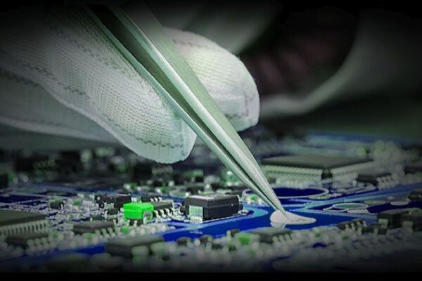
The objects that need to be cleaned after soldering are mainly the residues left on PCBs. According to the chemical properties, the leftover can be classified into three categories: water-soluble polar residues, water-insoluble non-polar residues and water-soluble but non-polar residues that can’t be changed into ionic organic compound. These contaminants are considered as the key cause leading to the change or even failure of PCB performance. Therefore, it’s extremely necessary to completely clean the residues. Additionally, PCBs are developing towards high-densification and fine-spacing, PCB cleaning is becoming especially important.
b. Fluxes
Flux residue accounts for the biggest part in PCB manufacturing, which is why the flux residue must be considered first when considering a type of cleaning craft. According to the chemical properties, fluxes can be classified into four categories by J-STD-004: rosin, resin, organic and inorganic, each of which is then classified according to flux/flux residue activity level and weight of halide. This also demonstrates from the side fact that all the fluxes in the world are capable of eliminating oxide, increasing the solder invasive capability.
In the process of PCB manufacturing, fluxes are used in wave soldering, reflow soldering and manual welding and it’s best to choose only one type of flux. For the cleaning of the whole PCB, it’s just a process of eliminating only one type of flux. If many types of fluxes are picked up, the compatibility of these fluxes will bring difficulties to cleaning since these fluxes have complicated characteristics that result in the complex of the combination of them.
c. Cleaning Craft
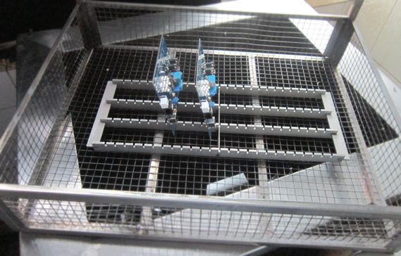
Three types of cleaning craft are ordinarily used in PCB cleaning: solvent cleaning, half-water cleaning and water cleaning. The solvent cleaning refers to the process in which solvent-type medium is used to clean PCBs. In this process, drying is carried out in independent equipment. Half-water cleaning refers to the process in which PCBs are cleaned by solvent and the organic solvent is cleaned off from the PCB by water in order to eliminate the flux and other contaminants on PCBs. Water cleaning refers to the process in which PCBs are cleaned only by water. According to the characteristics of equipment and products, suitable cleaning craft should be picked up so that the PCB reliability will be greatly increased.
d. Cleaning Solvent
According to the type of flux, cleaning solvent should be picked up compatible with the type of flux leftover. There are different types of cleaning solvents and the cleaning solvent components. Based on the regulations of Japan Industry Cleaning Committee (JICC), cleaning solvents are classified with the rinse process as a standard. That’s why cleaning solvents are classified into two types: water solubility cleaning solvent and non-water solubility cleaning solvent. The cleaning solvent with water used in the rinse process is called water solubility and without water used is called non-water solubility.
e. Cleaning Equipment and Cleaning Method
Nowadays cleaning equipments are mainly classified into batch type and cellular type while cleaning methods include ultrasonic, spray, immersion, jet, bubbles etc. Ordinary cleaning methods are carried out through spray or vapor phase, with some mechanical cleaning methods as supplement such as agitations, rotations etc.
f. Cleaning Standards
Different cleaning objects have different cleaning standards. Therefore, it is reasonable that the suitable cleaning standards must be compatible with the concerning industries and product characteristics since different products have different used environments, service lifespan, and different technical parameters.
According to the standards of IPC, the general highest cleaning grade is:
Ionic contaminants < 1.56μgNaCl/cm2;
or flux residue < 40μg/cm2;
or insulation resistance > 2×10⁶Ω.
All in all, as long as the PCB spot weld failure mechanism is fully understood concerning the bad effects of residues and suitable cleaning solvents and methods are chosen according to the cleaning craft design, the physical and chemical failure risk will be greatly decreased so that the reliability of PCB will be improved.
About the author:
Ming is the editor of PCBCart, an international custom PCB fabrication and assembly service supplier.
 If you enjoyed this article, you will like the following ones: don't miss them by subscribing to :