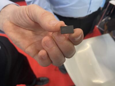
Researchers define ReRam switching characteristics
ReRAM memory chips or memristors have a number of properties that could make them strong contenders to existing technologies. Besides being very fast and energy-efficient, they scale very well and can be miniaturized well into the nanometer range. In contrast to today’s DRAMs, ReRAMs are non-volatile – they keep their data content even when they are switched off; booting computers could become a matter of milliseconds.
The function of memristive cells is based on a very specific physical effect: Their electric resistance is not constant but instead can be controlled through an external voltage. For instance, low resistance could be associated to a logical 1 while high resistance would be a logical 0.
At the physical level, the change of the electric resistance is caused by the movement of oxygen atoms: If they move out of the semi-conducting metal oxide layer, the material becomes conducting. Hitherto however the number of oxygen atoms to be moved to achieve the effect was widely unclear. Now the researchers at the Jülich Research Center succeeded in solving this question and explaining what actually is going on in such a memory cell during operation.
“Though first memristive memories are available at the market for some three years, their dimensioning was based widely on experience”, explains Regina Dittman from the Jülich Research Center’s Peter Grünberg Institute. According to Dittmann, the switching processes are occurring within tiny filaments. Such processes can be proved by photo emission microscopy, albeit this possibility was restricted to near-surface phenomena. The active area of ReRAM memory devices lies beneath a metal electrode and thus it so war was not possible to observe them during the switching process.
The solution to this problem lies in a material: Graphene. ”This nanomaterial forms a layer of carbon atoms that is just one atomic layer thick”, Dittmann explained. “Nevertheless it is just as conductive as a rather thick layer of metal. Since it is so thin we can look through it with our photo emission microscope.”
Experiments at the Bessy II synchrotron in Berlin in close cooperation with a working group around professor Claus Michael Schneider from the Peter Grünberg Institute were able to make the processes under the metal oxide layer visible and to exactly determine the variation of the carbon defect electrons within a filament during the instance of switching. Based on these findings, it was possible to create a computer simulation that determines the electrical characteristics of the component rather exactly. The results can be used for more realistic simulations in the future – and thus speed the development of commercial ReRam introduction.
Further reading: Quantifying redox-induced Schottky barrier variations in memristive devices via in-operando spectromicroscopy with graphene electrodes, Nature Communications (2016).
 If you enjoyed this article, you will like the following ones: don't miss them by subscribing to :
eeNews on Google News


