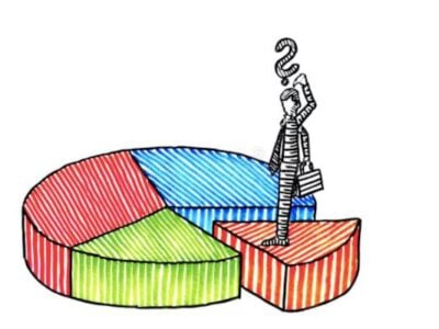
Temporary bonding equipment market to surf on the growth of thin wafer manufacturing
Indeed, ultra-thin wafers are less stable and more vulnerable to stresses, and die can be prone to breaking and warping—not only during grinding but also at subsequent processing steps. To address these challenges, as chip thickness is reduced, new processes including temporary bonding technologies will be required for handling such fragile wafers, specifically to support the wafer during back grinding and subsequent post-thinning processes. As tapes can no longer be used for ultra-thin wafers (main reasons are the non-uniformity of the tapes, adhesion and extreme flexibility), new wafer handling technologies have to be developed.
“We are at the very start of an impressive market growth for temporary bonding technology”, explains Dr. Eric Mounier, Project Manager at Yole Développement.
Many different approaches in development
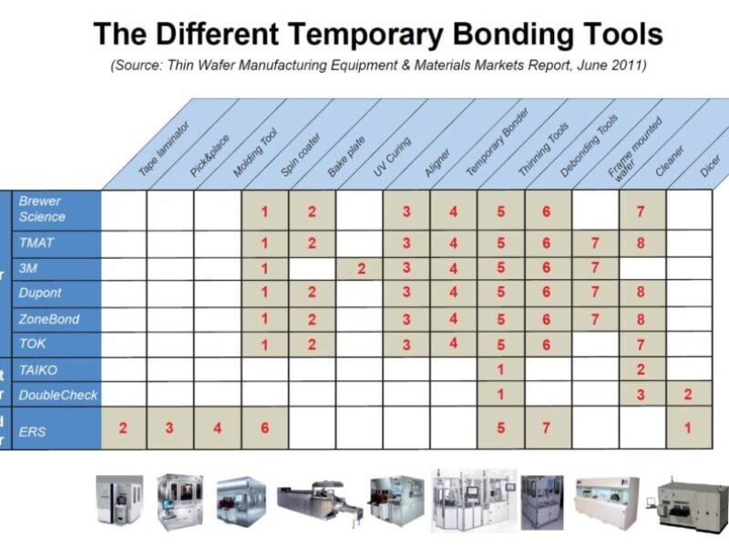
Temporary bonding technologies are numerous with no clear winning scenario coming out today, and the research firm has identified at least six different technologies for wafer temporary bonding with carriers. Each one of these approaches might have subtle differences in terms of chemistry, carriers and other attributes. Along with these approaches came also temporary bonding without carrier and reconstituted wafer for Fan Out WLP. So, the total number of approaches is more than 10 as of today. But this market is still in infancy and no clear temporary bonding technology is emerging. Many companies are competing to propose the best approach to achieve low cost, high temperature resistance and resolve topography issues.

As temporary bonding is a multi-disciplinary technology, it implies mastering know-how in process, chemistry and an understanding of the final application requirements. As a consequence, there are numerous collaborations running between tool makers, chemical players and substrate suppliers. Some companies are mastering both process and chemistry (Nitto Denko, TOK or TEL), but for others, partnerships are necessary. Temporary bonding is definitively a multiple-applications market. This is why the market is expected to boom. Yole Développement estimates the total number of wafers requiring temporary wafer bonding will be more than 35M by 2016 (all wafer sizes). Main applications driving temporary bonding are Advanced Packaging applications (TSV, interposers and Fan Out WLP), Power Devices (IGBTs), RF Devices & LEDs.
By 2016, Yole Développement evaluates the wafer temporary bonding (WTB) market equipment value for wafer & panels to be $300M by 2016.
Visit Yole Developpement at www.yole.fr
 If you enjoyed this article, you will like the following ones: don't miss them by subscribing to :